Scanning Electron Microscopy with Energy Dispersive X-Ray Analysis (SEM-EDS)
Scanning Electron Microscopy (SEM) is a powerful imaging technique that reveals detailed surface morphology and topography at the microscopic level. Combined with Energy Dispersive X-ray Spectroscopy (EDS), SEM provides critical insights into the elemental composition and distribution of materials. At CMG, we utilize SEM-EDS to deliver high-resolution imaging and precise material analysis for industries such as manufacturing, research, and quality control.
What is SEM-EDS?
SEM-EDS combines high-resolution imaging with elemental analysis to examine a material’s composition and structure. SEM produces detailed images of a material’s surface, while EDS identifies and quantifies the elements present by analyzing the unique X-rays emitted from the sample during electron beam irradiation.
Applications of SEM-EDS
- Elemental Composition: Identify which elements are present in a material, such as carbon, oxygen, silicon, or metals, to ensure material purity or detect contaminants.
- Elemental Distribution: Map where specific elements are located across the sample, useful for studying coatings, impurities, or heterogeneous materials.
- Quantitative Analysis: Measure the relative abundance of each element, essential for quality control in industries like semiconductors, pharmaceuticals, and alloys.
- Phase Analysis: Differentiate between material phases based on elemental composition, crucial for understanding properties in alloys, ceramics, or geological samples.
Advanced Capabilities with SEM-EDS
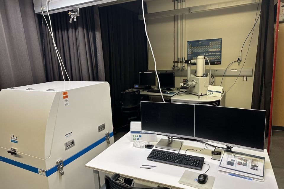
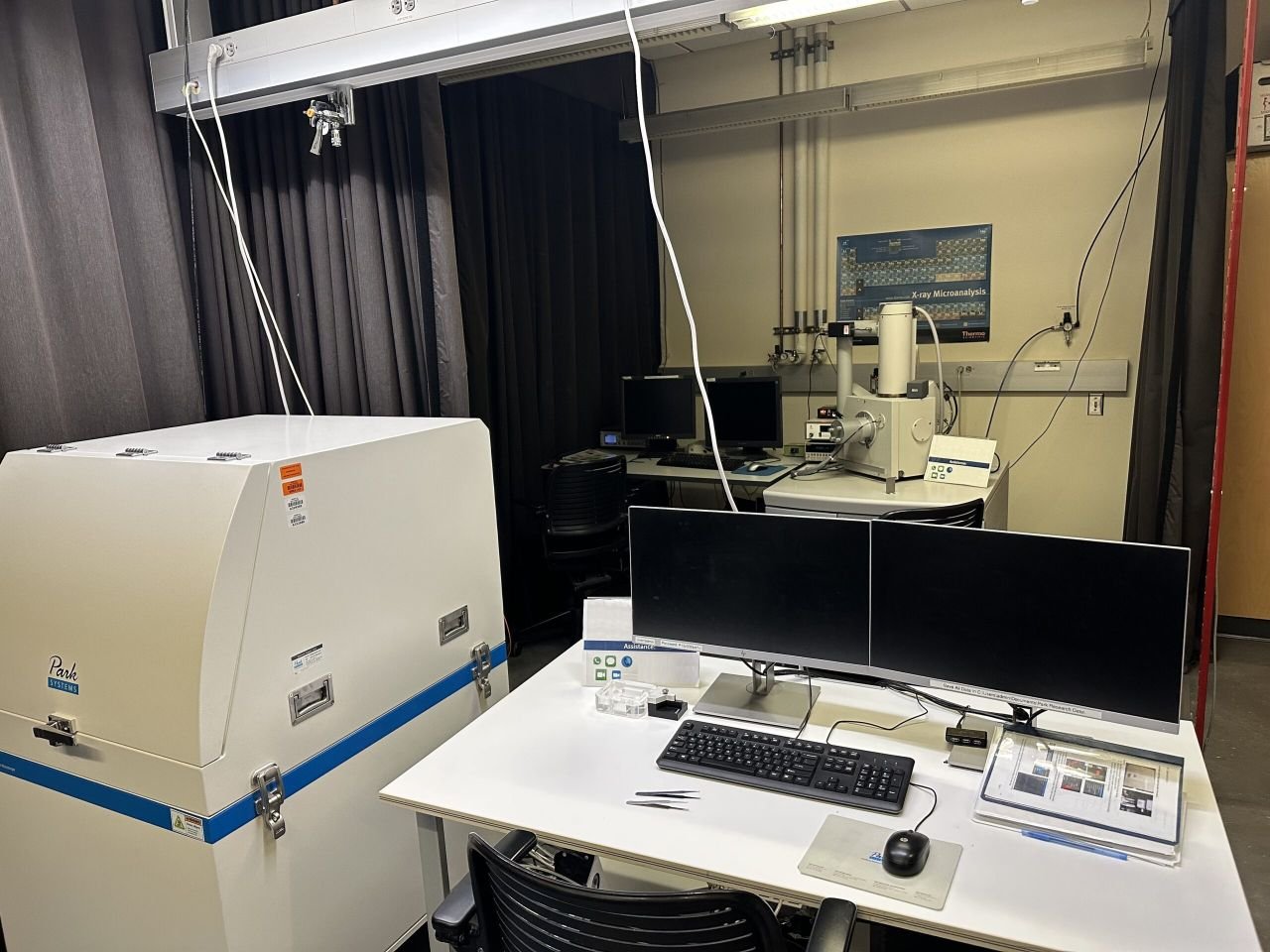
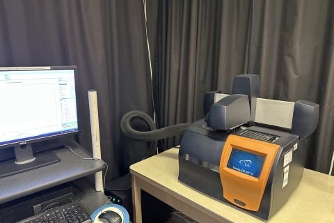
Modern SEM-EDS systems, such as ours Phenom XL Desktop SEM, enhance material characterization by:
- ChemiSEM Technology: Real-time elemental mapping directly over live SEM images for fast, intuitive analysis.
- Phase Mapping: Group regions with similar elemental compositions for deeper insight into a material’s microstructure.
- Efficiency: Seamless integration of imaging and analysis delivers results within minutes, ideal for high-throughput environments.
- Compact Design: The Phenom Desktop SEM fits easily into any lab, making it accessible to businesses and research institutions without requiring extensive infrastructure.
Why Use SEM-EDS?
SEM-EDS is invaluable for:
- Material science research.
- Failure analysis and quality control.
- Optimization of manufacturing processes.
- Development of advanced technologies like batteries, semiconductors, and coatings.
Why Choose CMG?
With cutting-edge SEM-EDS technology and experienced technicians, we provide high-resolution imaging and accurate elemental analysis tailored to your needs. Whether you’re identifying material defects, ensuring product quality, or advancing research, CMG delivers actionable insights to help you succeed.
Contact us today to learn more about our SEM-EDS capabilities.
